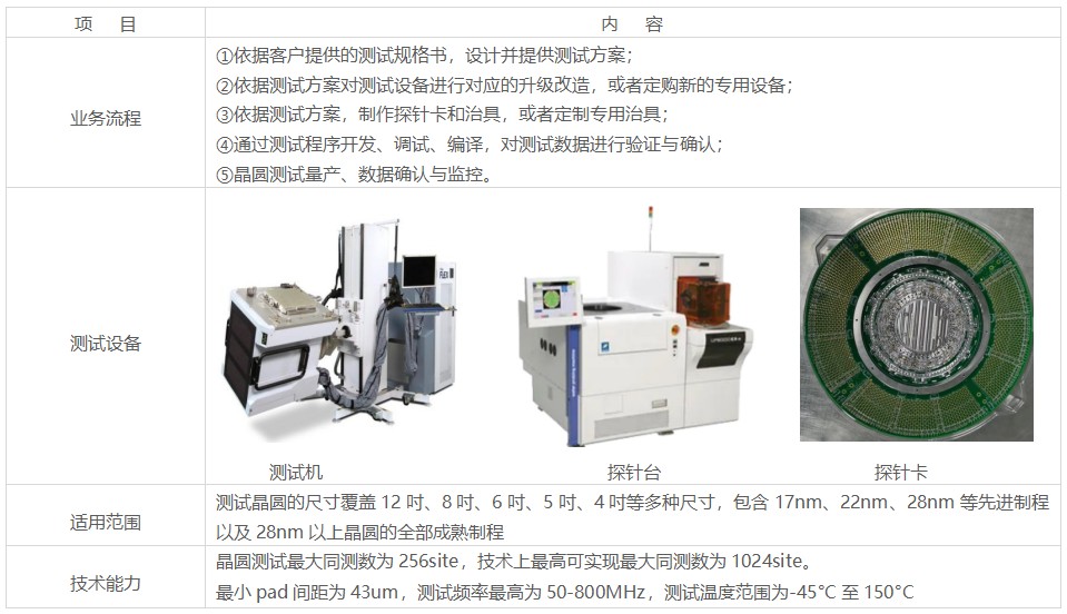
Wafer testing is a needle measurement of each grain on a wafer to test its electrical properties. During the test, the wafer is fixed on the tray of the probe, and the probe is in contact with each PAD point of the chip. The tester performs electrical and functional tests on the chip and records the results to distinguish the good ones from the bad ones. With 12″, 8″, 6″, 5″and 4″ wafer testing capabilities, including advanced processes such as 17nm, 22nm, 28nm and full mature processes for wafers above 28nm. Can test fingerprint identification, fire safety, Bluetooth, power management, MCU, filter, optical communication and many other application types.
Wafer testing process: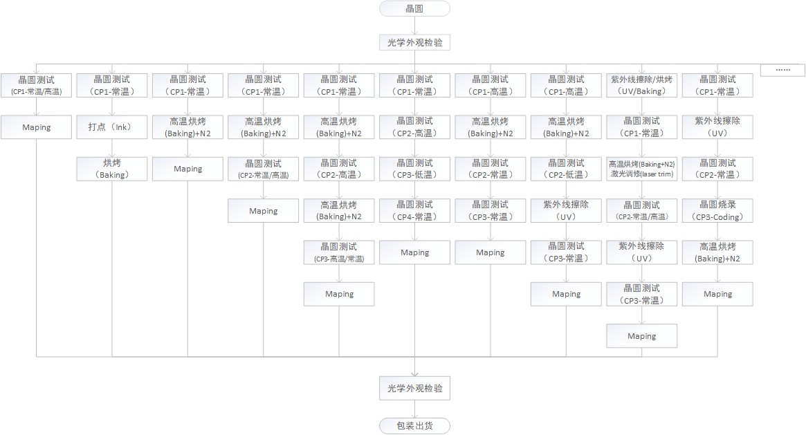
Testing machine:V93K、J750HD、D10、NI STS T4、S100、S50、STS8200、T862、TR6850S、TR6836S、Chroma3360D/3360P/3380、V50、TQT500、JC5600、SC312、T5503/5371、DST1000
Probe :UF3000、UF200SA
Wafer test MAPPING in BIN defines functions
Photoelectric chip, CMOS SENSOR test capability