About us
Company profile
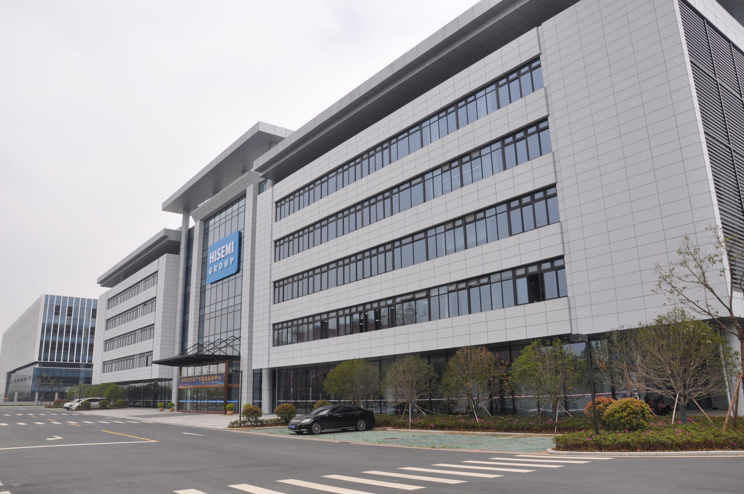
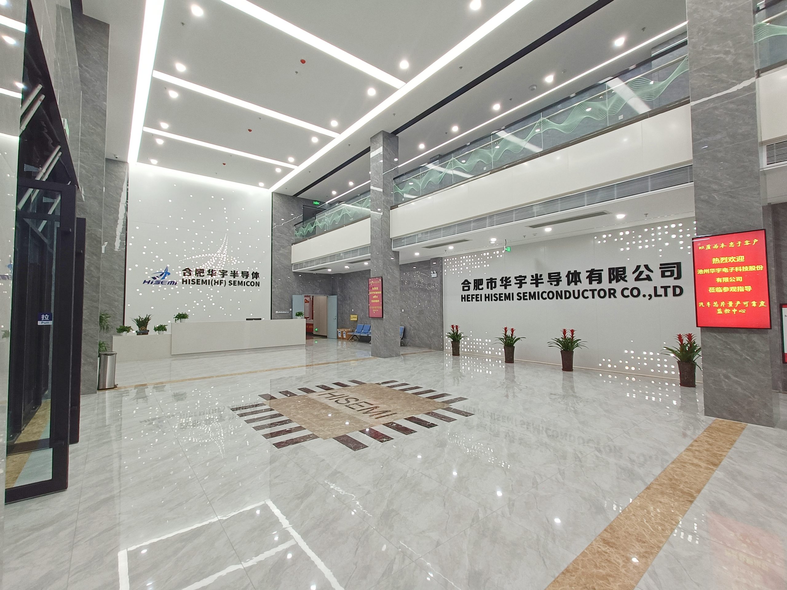
Hefei Hisemi Semiconductor Co., Ltd. was established in June 2021 with a registered capital of 50 million yuan, and is a wholly-owned subsidiary of Chizhou Hisemi Electronic Technology Co., Ltd. The company is a key investment attraction enterprise in Hefei in 2021, the main business is large-scale integrated circuit wafer testing, FT finished product testing and taping, is a high-tech private enterprise.
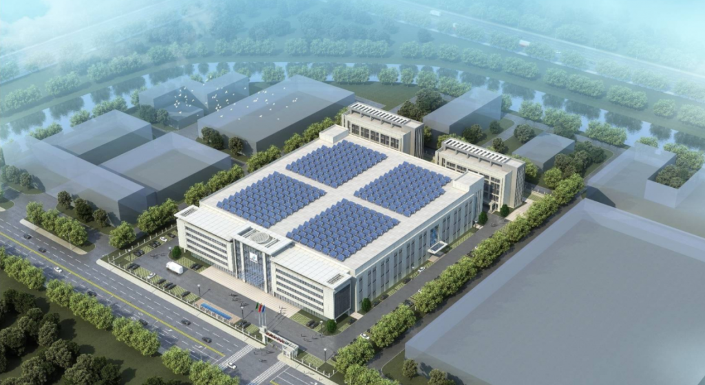
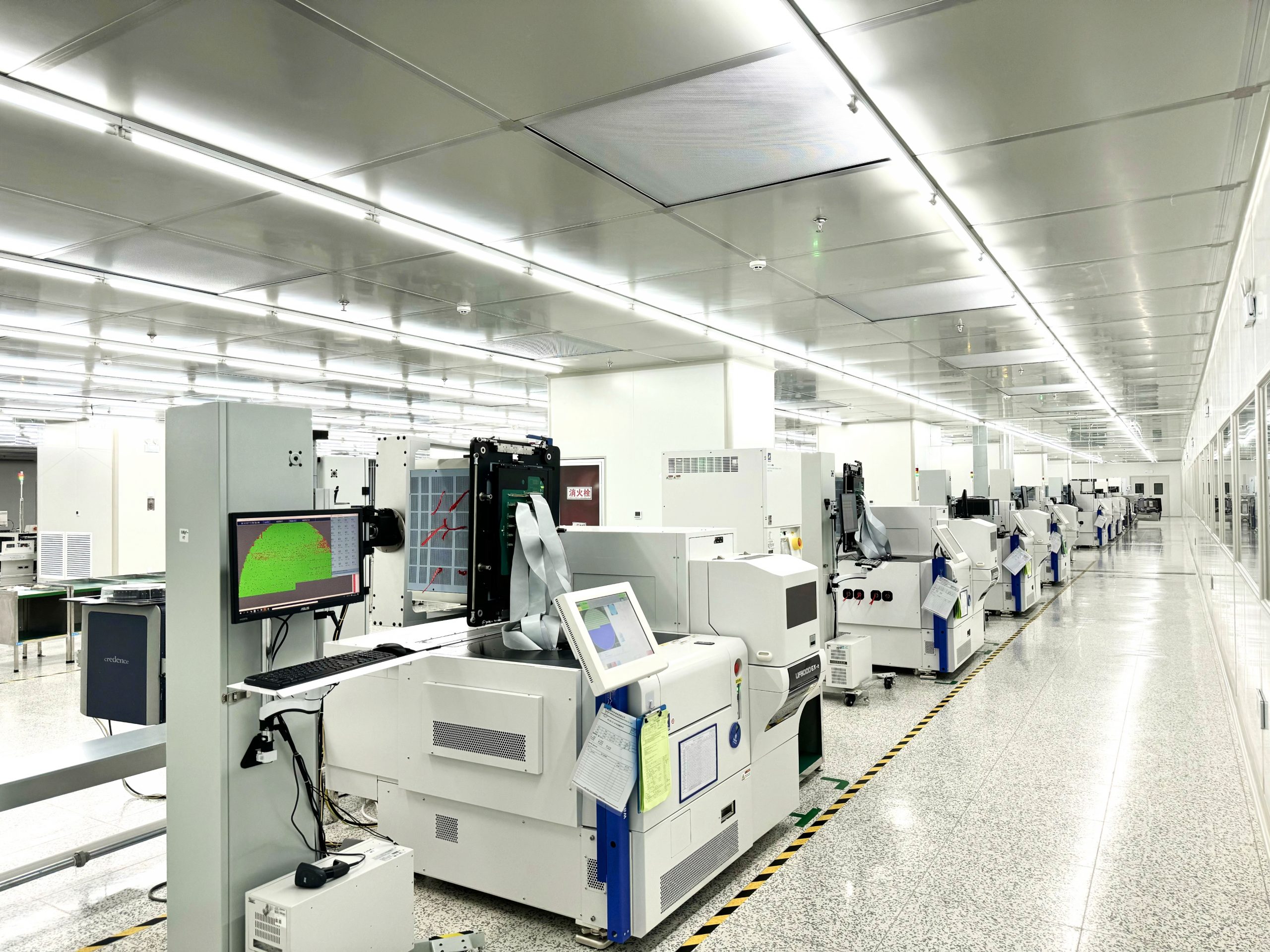
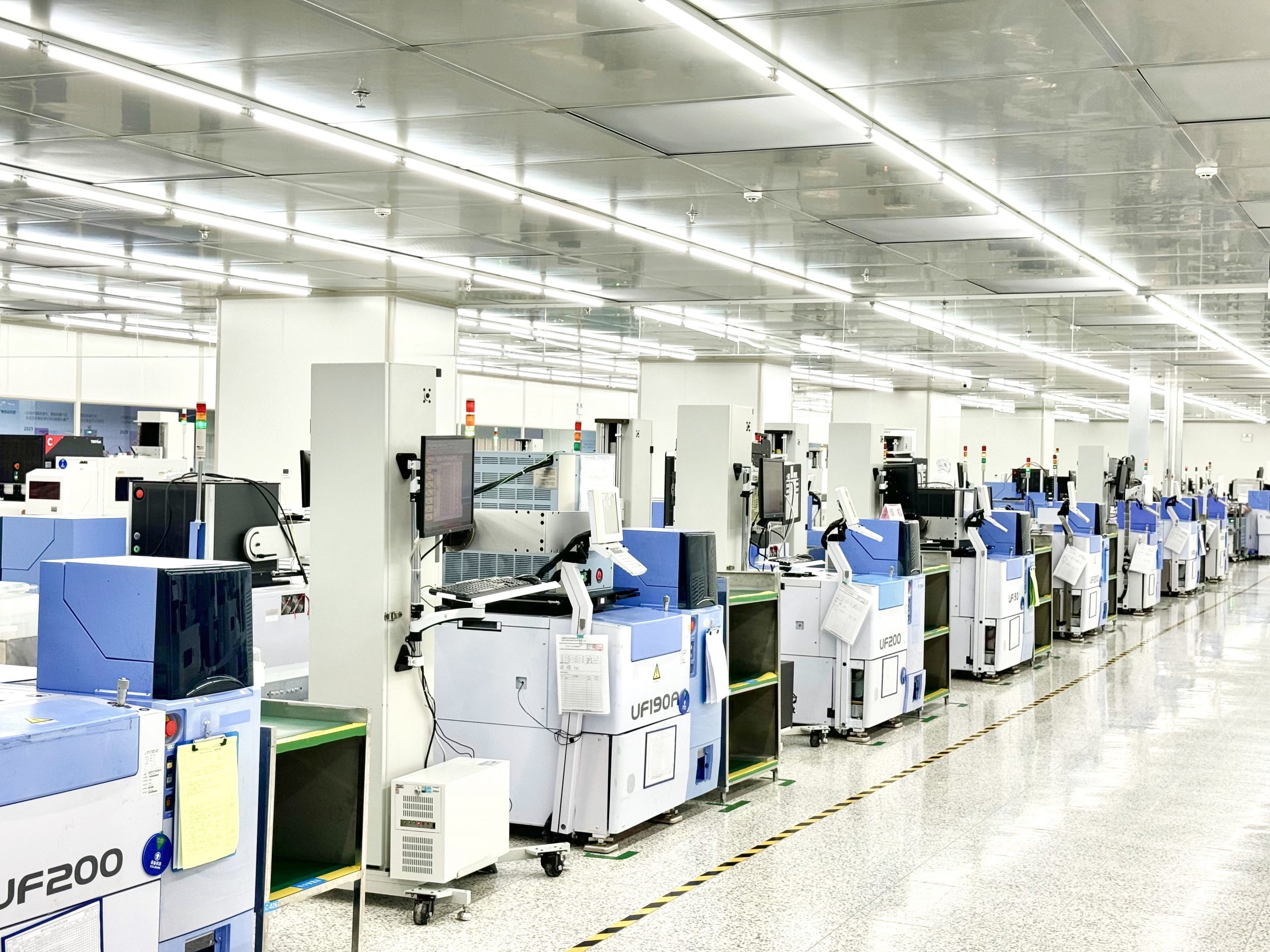
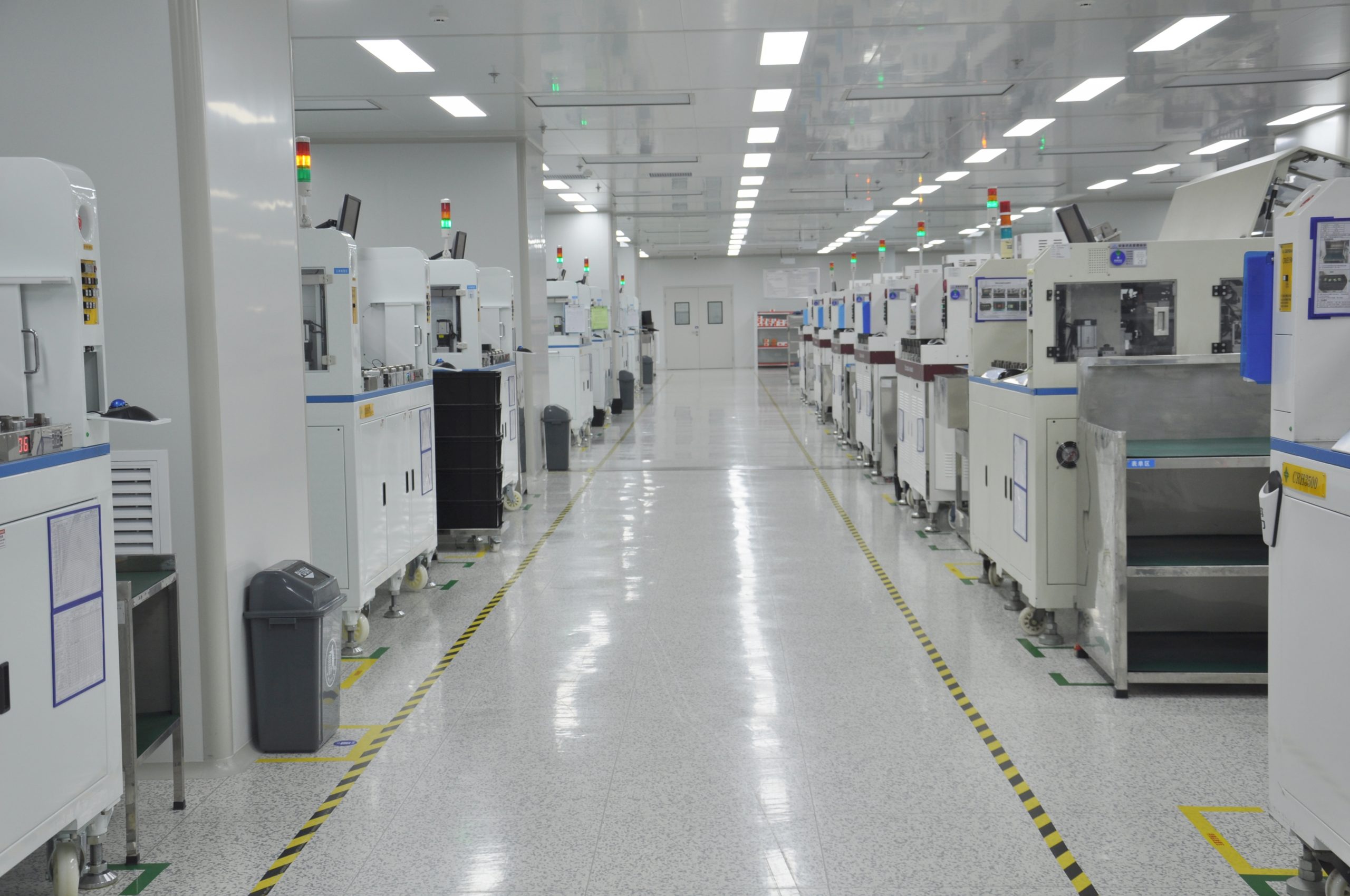
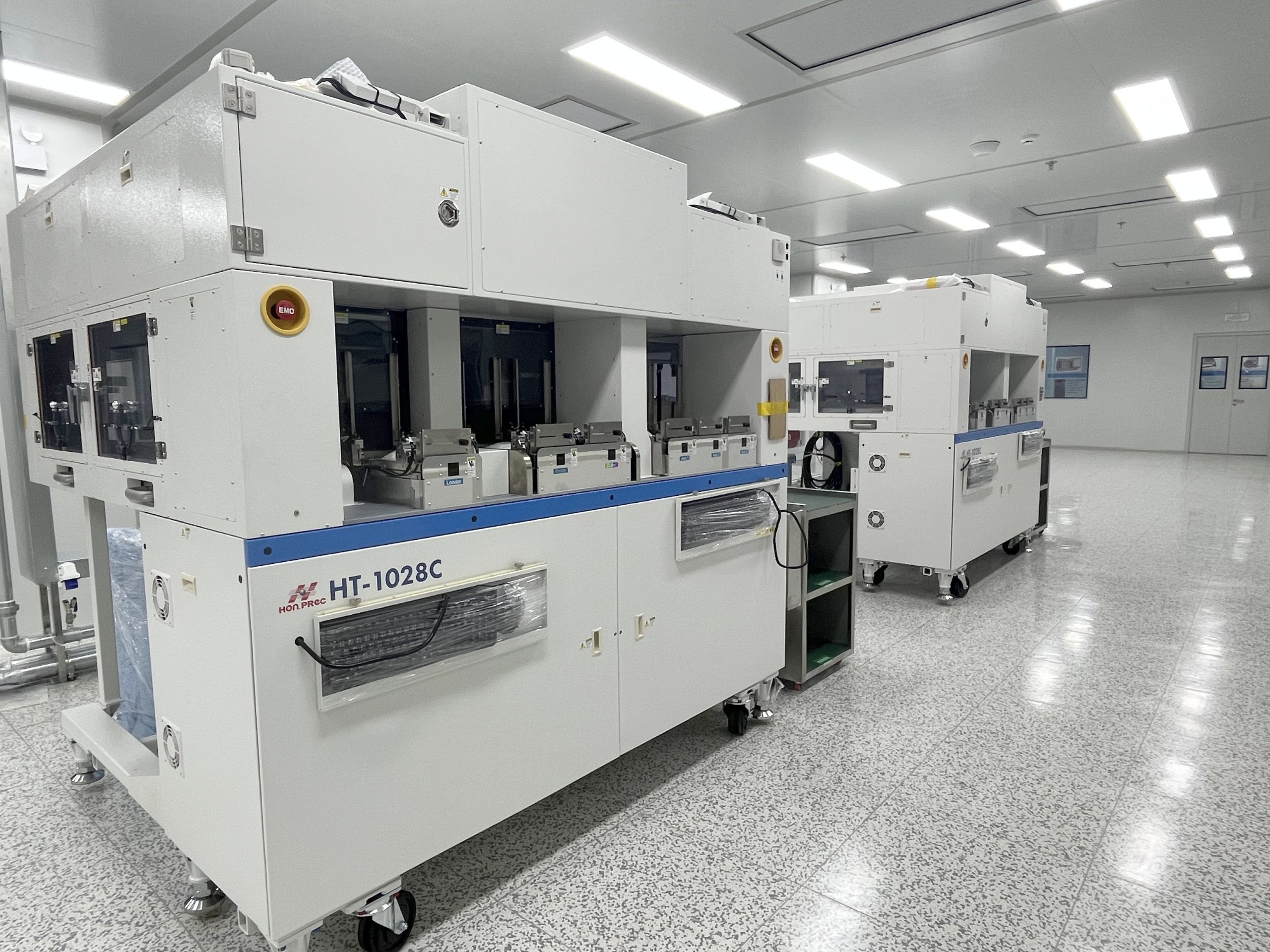
The company is now located in No. 66 Tiantangzhai Road, High tech Zone, Hefei City, Anhui Province, in the field of testing has formed a number of independent core technologies, the size of the test wafer covers 12 inches, 8 inches, 6 inches, 5 inches, 4 inches and other sizes, including 22nm, 28nm and above wafer process; In terms of chip finished product testing, the company has developed more than 30 chip test schemes such as MCU chips, ADC chips, FPGA chips, GPU chips, video chips, RF chips, SoC chips, digital signal processing chips, etc.; The company’s independent research and development of 3D taping machine, fingerprint recognition sorting equipment, gravity measurement and knitting machine and other equipment, has been used in actual production practice mature.